An Institute for Scalable Heterogeneous Computing
Summary
The future of computing innovation is becoming more uncertain as the 2020s have brought about a pivot point in the global semiconductor industry. We owe this uncertainty to several factors, including the looming end of Moore’s Law, disruptions in semiconductor supply chains, international competition in innovation investment, a growing demand for more specialized computer chips, and the continued development of alternate computing paradigms, such as quantum computing.
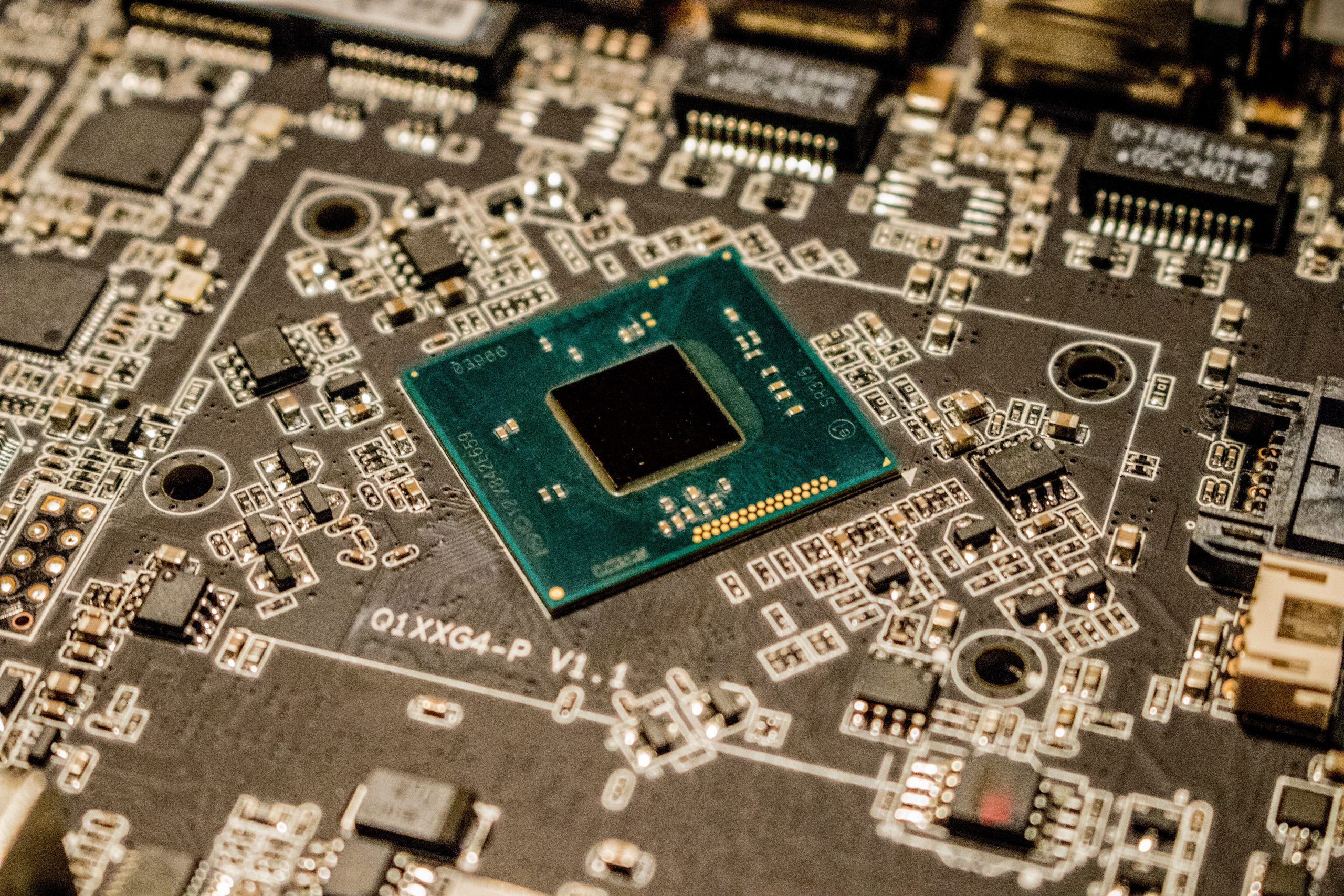
In order to address the next generation of computing needs, architectures are beginning to emphasize the integration of multiple, specialized computing components. Within this framework, the U.S. is well poised to emerge as a leader in the future of next-generation computing, and more broadly advanced semiconductor manufacturing. However, there remains a missing link in the United States’ computing innovation strategy: a coordinating organization which will down-select and integrate the wide variety of promising, next-generation computing materials, architectures, and approaches so that they can form the building blocks of advanced, high-performance, heterogeneous systems.
Armed with these facts, and using the existing authorization language in the 2021 National Defense Authorization Act (NDAA), the Biden Administration and Congress have a unique opportunity to establish a Manufacturing USA Institute under the National Institute of Standards and Technology (NIST) with the goal of pursuing advanced packaging for scalable heterogeneous computing. This Institute will leverage the enormous body of previous work in post-Moore computing funded by the federal government (Semiconductor Technology Advanced Research Network (STARnet), Nanoelectronics Computing Research (nCORE), Joint University Microelectronics Program (JUMP), Energy-Efficient Computing: From Devices to Architectures (E2CDA), Electronics Resurgence Initiative (ERI)) and will bridge a key gap in bringing these R&D efforts from the laboratory to real world applications. By doing this, the U.S. will be well positioned to continue its dominance in semiconductor design and potentially regain advanced semiconductor manufacturing activity over the coming decades.
At the Office of Clean Energy Demonstrations, Dr. Glaser is paving the way for cutting-edge energy storage and battery technologies to scale up.
Outside of loans, the federal government can do more to support the restart and ensure other nuclear plants continue generating clean baseload energy for as long as safely possible.
The ongoing failure of the U.S. to invest comes at a time when our competitors continue to up their investments in science.
Science funding agencies are biased against risk, making transformative research difficult to fund. Forecast-based approaches to grantmaking could improve funding outcomes for high-risk, high-reward research.